Background
An organic TFT (thin film transistor) can be manufactured at a relatively low temperature, so it can be formed on a flexible plastic substrate. TFTs are strong candidates as transistors for thin, light computer displays.
Pentacene has attracted attention as a material having a mobility close to that of amorphous silicon (Si). Mobility can be further enhanced by controlling the crystal phase and molecular orientation.
Investigation
To identify crystal phases and evaluate molecular orientation, X-ray diffraction measurements were performed on different thicknesses (150 nm and 20 nm) of polycrystalline pentacene thin films formed under different conditions on a heated 300 nm thick oxide film on a Si (001) substrate under an ultrahigh vacuum using the MBE method. Out-of-plane and in-plane measurements1 were performed using Rigaku's SmartLab multipurpose diffractometer.
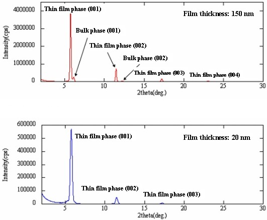
In both samples, only the diffraction lines of pentacene (00l) series were observed, suggesting that the molecules of these samples are oriented. For the 150 nm thick sample, not only the diffraction lines of thin film phases with the c-axis length of 15.40 Å but also the diffraction lines of bulk phases with the c-axis length of 14.40 Å were observed3. In addition, For the 20 nm thick sample, the diffraction lines of thin film phases were observed, but the diffraction lines of bulk phases were not.

The widths of the rocking curves for the thin film phases are about 0.08° to 0.09°, roughly the same value irrespective of the difference of the film widths, revealing that they have very high orientations. The widths of the rocking curves for the bulk phases are about 0.22°, revealing that there is a difference in the orientation according to the phase.

In the in-plane measurement, diffraction profiles with good S/N ratios that are not disturbed by the signals from the thermally-oxidized film and the Si substrate were obtained, and from both samples the diffraction lines of pentacene (hk0) components were observed. As for the out-of-plane measurement, the thin film and bulk phases were observed for the 150 nm thick sample. Using the pentacene (110) diffraction line of the thin film phase at 2θ = 19°, the crystallite size of the thin film phase was estimated using the Scherrer formula, obtaining about 50 nm for both samples. (Samples were provided by: Saiki Laboratory, Department of Complexity Science and Engineering, Graduate School of Frontier Sciences, University of Tokyo.)
References:
- Katsuhiko Inaba, Rigaku J. 35 27-36 (2004)
- C.C. Mattheus, et al., Acta Crystallogr. Sec. C, 57 939-941 (2001)
- J.S. Wu and J.C.H. Spence, J. Appl. Crystallogr. 37 78-81 (2004)