Background
ZnO is a II-VI semiconductor and its features include good transparency, high electron mobility, and wide bandgap etc. Its applications as thin film transistors (TFT) and light emitting diodes (LED) have been studied recently as well as its use as additives to plastics, ceramics, etc. and transparent electrodes. For those relatively new applications, an epitaxially grown ZnO is required and it is important to characterize how the films are grown on the substrate by determining its major orientation and checking if there are any other minor orientations. The combination of the in-plane and out-of-plane techniques is useful for the study of epitaxial film orientations. Those two techniques provide orientation information in two directions which are perpendicular and parallel to the surface, respectively. Since you can see those two directions directly, the interpretation of the data is more intuitive than the conventional technique that uses the asymmetric reflections that are from lattice planes tilted from the surface.
Investigation
Figure 1 shows a set of in-plane and out-of-plane scans from ZnO film on a c-axis sapphire substrate collected on the SmartLab X-ray diffractometer with the in-plane arm. The phi scan which is sample in-plane rotation at ZnO (100) is also shown in Figure 2.
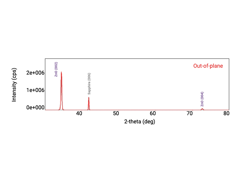
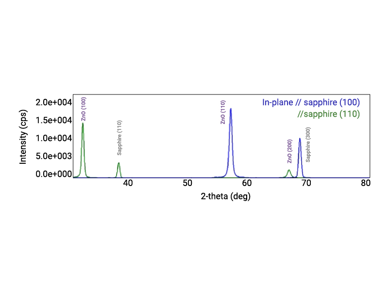
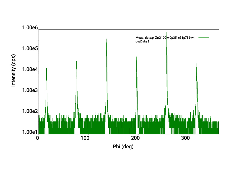
The scans in Figure 1 show that the ZnO was grown with its c axis parallel to the sapphire c axis and its a axis rotated 30° from the sapphire a axis as shown in Figure 3. The phi scan in Figure 2 shows six-fold symmetry and this indicates that the ZnO film is a single domain epitaxial film and there are no other orientations.
