
Semiconductors
X-ray metrology solutions from lab to fab
Semiconductors have the power to change the world for the better. Rigaku strives to make this a reality as the leading global supplier of X-ray metrology tools for semiconductor process R&D and high-volume manufacturing.
Rigaku is a leading manufacturer of X-ray technology-based instruments that solve manufacturing challenges in semiconductor R&D and production. With over 70 years of global market leadership, our advanced families of products provide solutions for everything from in-fab process control metrology to R&D for thin film and materials characterization.


AZX 400
WDXRF sequential spectrometer for light-element and metal film thickness and composition measurements for up to 400 mm coupons, sputtering targets, and wafers
Learn more
WDA-3650
WDXRF simultaneous spectrometer for light-element and metal film thickness and composition measurements on wafers and media disks for up to 200 mm wafers
Learn more
WaferX 310
WDXRF simultaneous spectrometer for thickness and composition measurements for up to 300 mm wafers
Learn more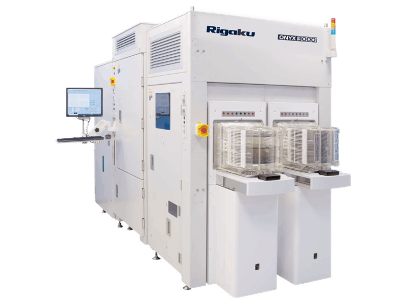
ONYX 3000
EDXRF and optical hybrid metrology tool for automated X-ray analysis, 3D scanning, and 2D microscope for film thickness and composition measurements on blanket and patterned wafers for up to 300 mm wafers
Learn more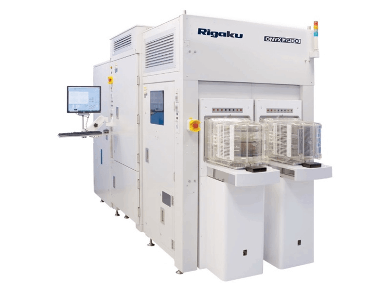
ONYX 3200
EDXRF and optical hybrid metrology tool for automated X-ray analysis, 3D scanning, and 2D microscope for film thickness and composition measurements on blanket and patterned wafers for up to 300 mm wafers
Learn more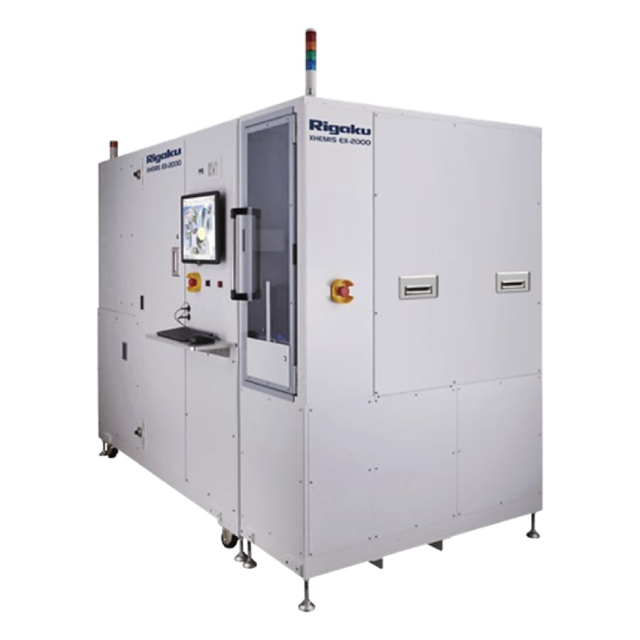
XHEMIS EX-2000
Enables high-throughput measurements on blanket wafers ranging from ultra-thin single-layer films to multilayer stacks for process development and film quality control.
Learn more
XTRAIA MF-3000
XRR, EDXRF, and XRD metrology tool for composition and thickness (EDXRF), thickness, density, and roughness (XRR) for unpatterned and patterned films for up to 300 mm wafers
Learn more
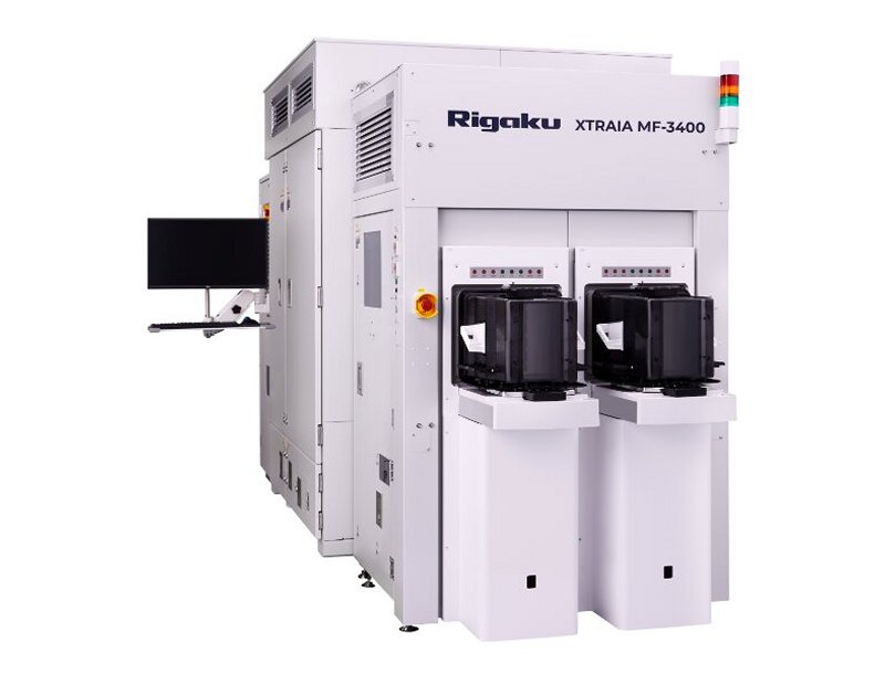
XTRAIA MF-3400
Multi-functional XRR / XRD / XRF metrology system for thin-film analysis and process control for patterned wafer up to 300 mm.
Learn more
XTRAIA MF-2000
XRR, EDXRF, and XRD metrology tool for composition and thickness (EDXRF), thickness, density, and roughness (XRR) for unpatterned and patterned films for up to 200 mm wafers
Learn more

XHEMIS TX-2000
Next-generation total-reflection XRF system for surface-metal control in semiconductor fabs for wafers up to 200 mm
Learn more
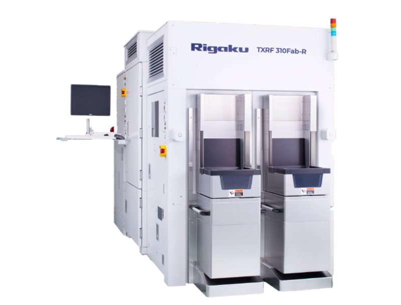


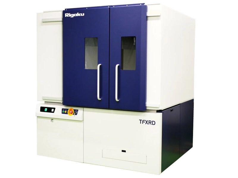
TFXRD Lab
HRXRD and XRR system for thickness, density, roughness, composition, strain, relaxation, and RSM characterization of unpatterned epitaxial films with full-wafer mapping capability for near-fab applications for up to 300 mm wafers
Learn more
TFXRD Near Fab
HRXRD and XRR system for thickness, density, roughness, composition, strain, relaxation, and RSM characterization of unpatterned epitaxial films with full-wafer mapping capability for near-fab applications for up to 200 mm wafers
Learn more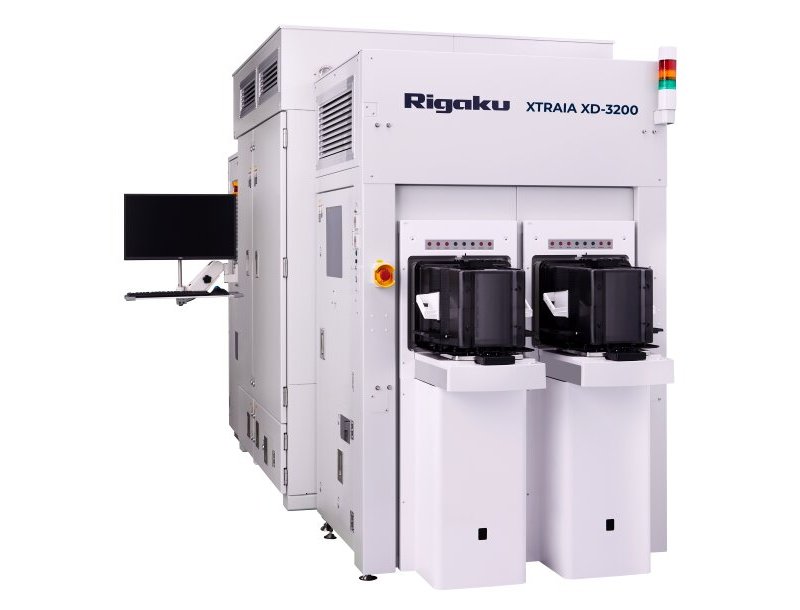
XTRAIA XD-3200
HRXRD and XRR metrology tool for thickness, density, roughness, composition, strain, relaxation, and RSM characterization of unpatterned epitaxial films for up to 300 mm wafers
Learn more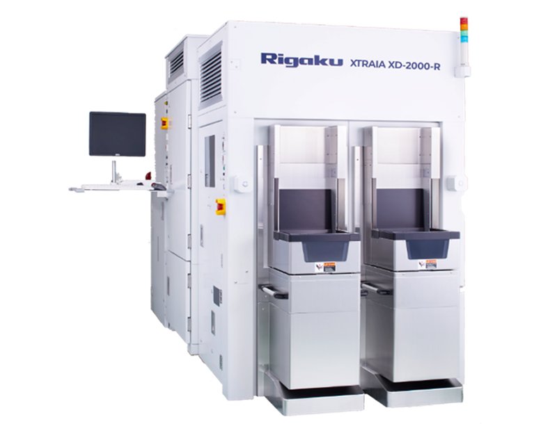
XTRAIA XD-2000R
Non-destructive X-ray reflectometry metrology tool for multilayer films, EUV masks, and advanced thin-film applications.
Learn more
XTRAIA XD-3300
XTRAIA XD-3300 HRXRD and XRR metrology tool for thickness, density, roughness, composition, strain, relaxation, and RSM characterization of unpatterned and patterned epitaxial films for up to 300 mm wafers
Learn more
XTRAIA CD-3200T
TSAXS metrology tool for critical dimension (CD) and profile shape characterization of deep (high aspect ratio) structures for 300 mm wafers
Learn more
XTRAIA CD-3010G
GISAXS and XRR metrology tool for critical dimension (CD) and profile shape characterization of shallow structures and XRR characterization of film thickness, density and roughness for 300 mm wafers
Learn more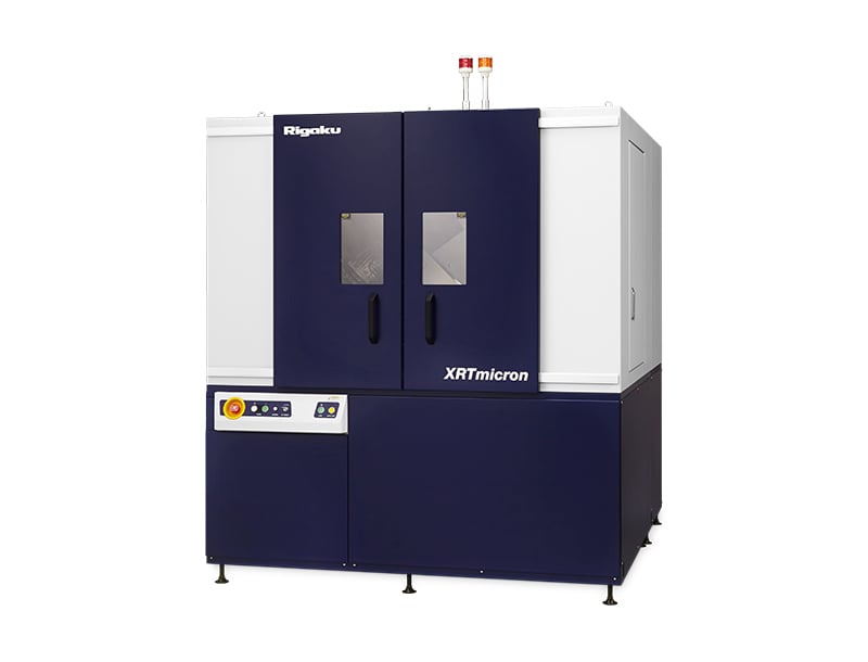
XRTmicron (Lab)
XRT (X-ray topography) imaging system for emerging power electronics, optoelectronics, and 5G / 6G communications (SiC, GaN, GaAs, InP, Ga₂O₃) for up to 300 mm wafers
Learn more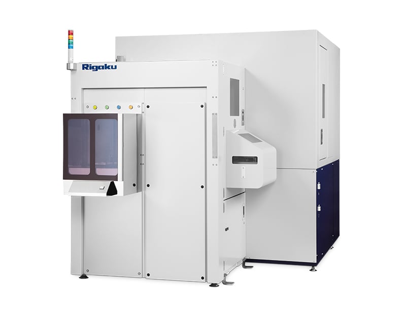
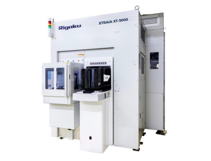
XTRAIA XT Series (Fab)
High-resolution, non-destructive wafer defect visualization for semiconductor manufacturing
Learn more
XTRAIA TF Series
High-resolution, non-destructive full-wafer characterization for thin film manufacturing
Learn more
FSAS II
XRD system for measurement and control of crystal orientation for up to 150 mm wafers, ingots
Learn more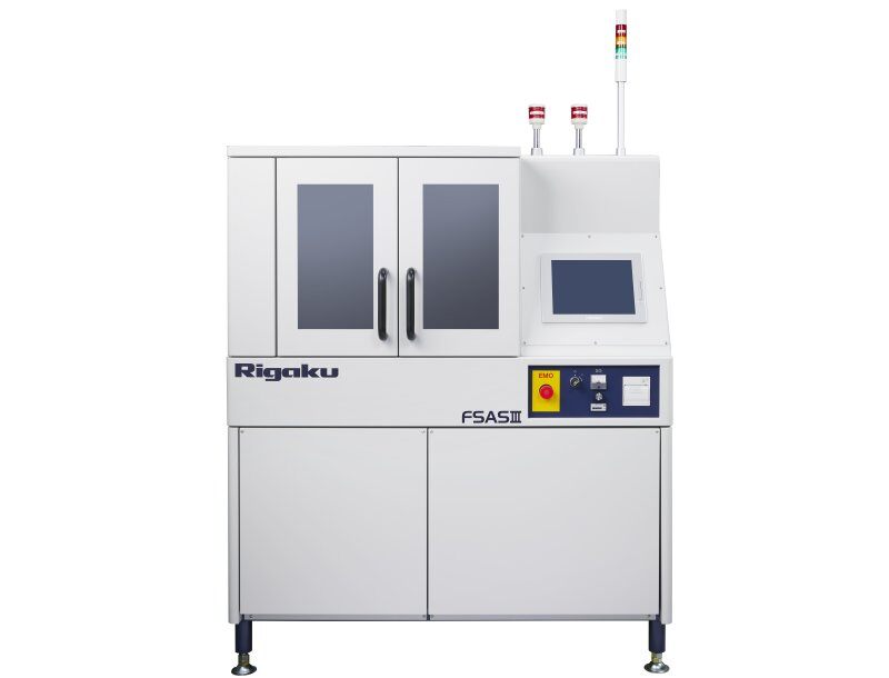
FSAS III
XRD system for measurement and control of crystal orientation for up to 150 mm wafers, ingots
Learn more
SmartLab
Advanced, state-of-the-art, high-resolution XRD system powered by Guidance expert system software
Learn more
Contact Us
Whether you are interested in getting a quote, want a demo, need technical support, or simply have a question, we're here to help.