
What Is High-resolution XRD Used For?
Epitaxial lattice parameter measurements
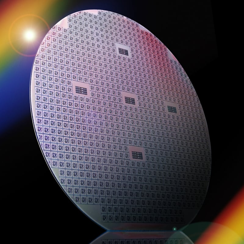
X-ray diffraction is especially valuable to the study of epitaxial layers and other thin film materials. Using precision lattice parameter measurement methods, the lattice mismatch of an epitaxial layer and its substrate can be determined with great precision. This lattice parameter match or mismatch is an important factor in epitaxial devices such as magnetic garnet films for bubble memories, doped gallium arsenide films for LED and high-speed transistors, infra-red detectors and other important electronic products. Another interesting use of XRD for thin films is that the coefficient of thermal expansion can be determined by plotting lattice parameters versus temperature using a high temperature diffractometer.
High-resolution X-ray rocking curves are often used to determine precisely the composition and thickness of epitaxial alloy films. These pieces of information can be obtained by simulating and/or fitting the measured rocking curve using X-ray dynamical diffraction theory.Rigaku's SmartLab diffractometer, which offers variable resolution optics, is ideal for such purposes. The modular design of the SmartLab optics allows users to easily insert different optical elements of their choice, such as Ge(220)x2, Ge(220)x4, Ge(400)x2, or Ge(440)x4 monochromators for the incident beam and a Ge(220)x2 analyzer for the diffracted beam. These optic modules can be automatically detected by the controlling computer and are aligned automatically. An automatic variable receiving slit is also available for the diffracted beam.
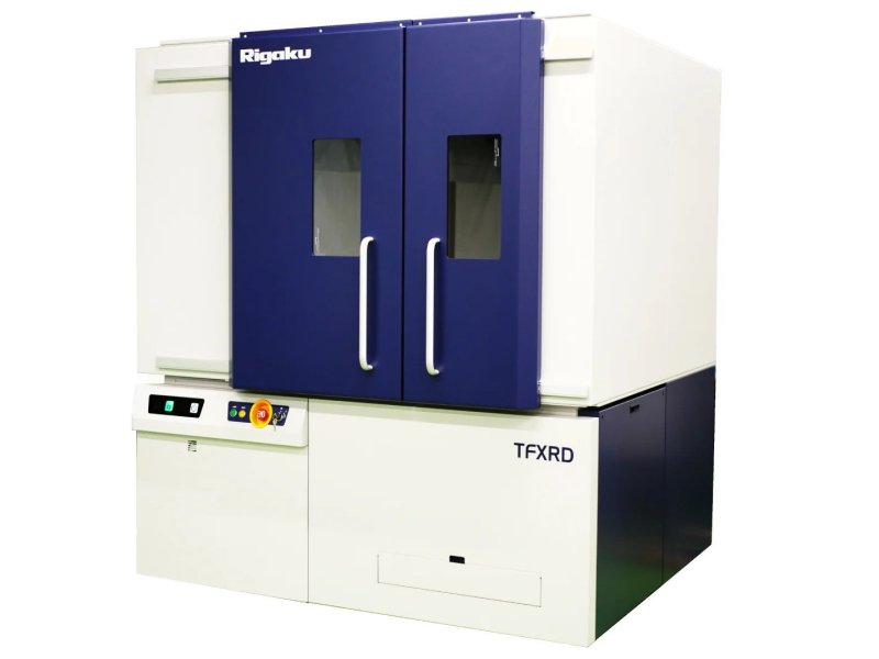
TFXRD Lab
HRXRD and XRR system for thickness, density, roughness, composition, strain, relaxation, and RSM characterization of unpatterned epitaxial films with full-wafer mapping capability for near-fab applications for up to 300 mm wafers
Learn more
TFXRD Near Fab
HRXRD and XRR system for thickness, density, roughness, composition, strain, relaxation, and RSM characterization of unpatterned epitaxial films with full-wafer mapping capability for near-fab applications for up to 200 mm wafers
Learn more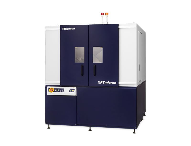
XRTmicron (Lab)
XRT (X-ray topography) imaging system for emerging power electronics, optoelectronics, and 5G / 6G communications (SiC, GaN, GaAs, InP, Ga₂O₃) for up to 300 mm wafers
Learn more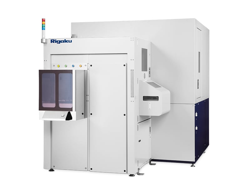
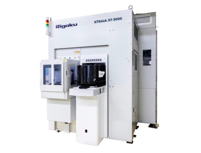
XTRAIA XT Series (Fab)
High-resolution, non-destructive wafer defect visualization for semiconductor manufacturing
Learn more
XTRAIA TF Series
High-resolution, non-destructive full-wafer characterization for thin film manufacturing
Learn more
SmartLab
Advanced, state-of-the-art, high-resolution XRD system powered by Guidance expert system software
Learn more
SmartLab SE
Highly versatile multipurpose X-ray diffractometer with built-in intelligent guidance
Learn more
Rigaku Automation Interface
Open Python orchestration interface for seamless integration and safe testing
Learn more
Contact Us
Whether you're interested in getting a quote, want a demo, need technical support, or simply have a question, we're here to help.