ONYX 3000


Features
- Micro-spot X-ray beam and pattern recognition
- 2D- and 3D- optical characterization of device structures
- High-throughput, blanket- and product-wafer measurements
- Wide range of materials and applications
- High resolution and precision covering thicknesses from Ångstroms to microns
- Helium purged measurement environment for light-element sensitivity
- Configurable for 300mm and smaller wafers
- Design based on SEMI S2 and SEMI S8
Hybrid XRF and Optical metrology FAB tool
Thickness, composition, defect identification and sizing of films and structures on blanket and patterned wafers
Specifications
| Product name | Onyx |
| Technique | X-ray fluorescence and optical microscopy |
| Benefit | Measure ultra-thin single-layer films to multi-layer stacks; Characterize BEOL and WLP structures |
| Technology | Process micro-spot EDXRF and 2D-, 3D- optical microscopy |
| Core attributes | Design based on SEMI S2 and SEMI S8, micro-spot polycapillary X-ray optics |
| Core options | SECS/GEM communication software, COLORS beam modules |
| Computer | Internal PC, MS Windows® OS |
| Core dimensions | 1390 (W) x 2040 (H) x 2960 (D) mm |
| Mass | ~1250 kg |
| Power requirements | 1Ø, 208 VAC 50/60 Hz, 16A |
Applications

Single Bump Metrology
Measure and monitor Ag%, Sn%, Ni layers, Cu thickness, and total bump height:- Measure single-solder bumps as small as 10 μm diameter
- Inspect a range of parameters: across the wafer, wafer-to-wafer, and lot-to-lot
- Measure CD and a total height of single bumps using a 2D microscope, 3D scanner, and built-in sensors
Thin Films Measuring and Monitoring
Measure and monitor thickness and composition of precious metal thin films:- Analyze ultra-thin films of any type of element, regardless of their physical properties

UBM/RDL
Conduct metallurgical inspections of under bump metallization (UBM) and redistribution layers (RDL):- Analyze multi-stack structures and thick monolayers, for layer thickness and composition
- Distinguish separate layers simultaneously
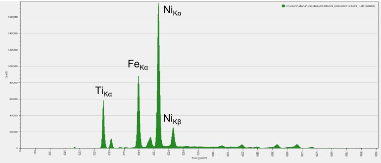
Alloy Compositions
Measure and monitor metals and alloy composition:- Analyze metal elements (Ga, P, Co, Ni, Fe, Pt, Cr, Zn, and Mn)
- Identify alloys (NiFe, CoNi, NiP, NiPt, and CrMn)