X-ray Topography Systems
 X-ray topography from Lab to Fab
High-resolution, non-destructive wafer defect imaging for every stage of semiconductor manufacturing
- Three configurations: Lab, Near-Fab, and Fab systems for seamless R&D to production scaling
- Up to 300 mm wafers with full-wafer, non-destructive defect detection
- Multi-material support: Si, SiC, GaN, InP, GaAs, AlN, Ga₂O₃, Sapphire, and more
- SEMI-compliant QC tools for TSD, BPD and MP quantification in SiC
The XRTmicron Series is Rigaku’s high-resolution X-ray topography (XRT) platform, designed to detect and quantify crystallographic defects across single crystalline materials such as semiconductor wafers and epitaxial layers on wafers. With configurations tailored for R&D labs, pilot lines, and full-scale fabs, XRTmicron enables end-to-end defect visualization and yield optimization across the semiconductor value chain. By combining non-destructive measurement, cleanroom compatibility, and advanced automation, the XRTmicron Series delivers accurate defect maps and statistical analysis of dislocations. It bridges the gap between research innovation and manufacturing reliability, empowering fabs to accelerate development, optimize crystal growth, and secure long-term device performance.
 Features
- Dual measurement modes: Transmission and Reflection imaging in one system
- X-ray sources and optics dedicated for topography : High-brilliance dual-wavelength MicroMax-007 with parabolic multilayer mirrors
- Detector options:
- XTOP (5.4 μm/pixel) high-resolution imaging
- HR-XTOP (2.4 μm/pixel) ultrahigh resolution (optional)
- HyPix-3000HE (100 μm/pixel) for high-speed scans
- 3D cross-section topography for defect localization through wafer thickness
- XRT Toolbox software: Defect mapping, SEMI-compliant reporting (M91/M93), KLARF export, batch analysis, automated calibration
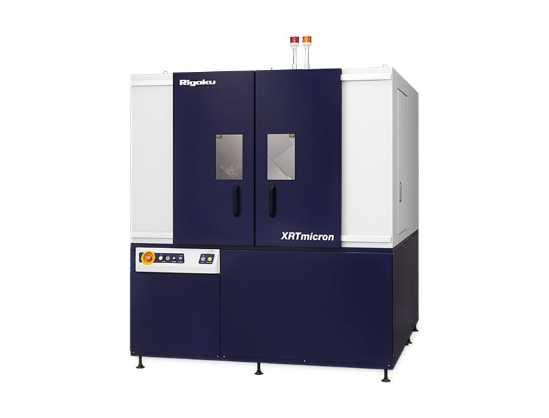
XRTmicron (Lab)
- Compact configuration for research and early development
- Manual wafer and sample handling
- Supports wafers up to 300 mm and crystal ingots/boules
- Ideal for academic labs, R&D centers, and material suppliers
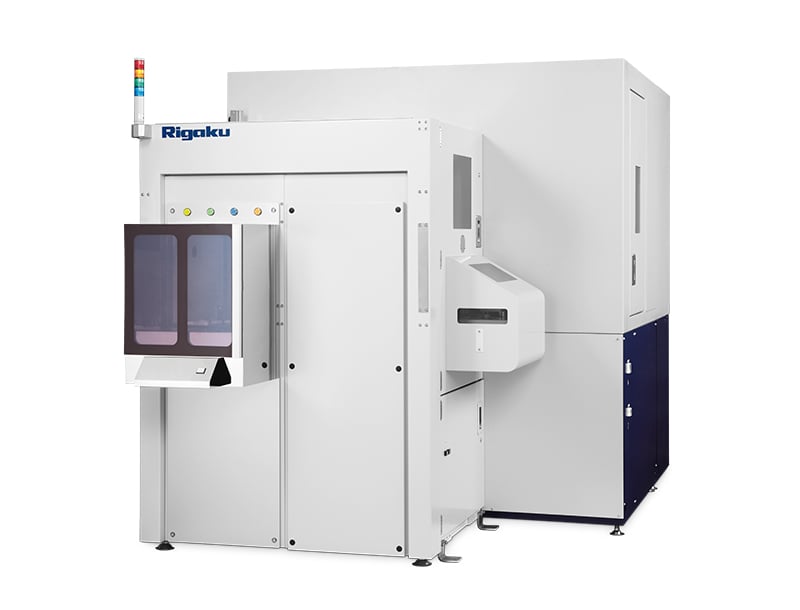
XRTmicron (Near-Fab)
- Hybrid solution for R&D and pilot-line integration
- Automated and manual wafer transfer available
- Supports 75–300 mm wafers with multiple holder options
- Bridges process development and in-line quality control
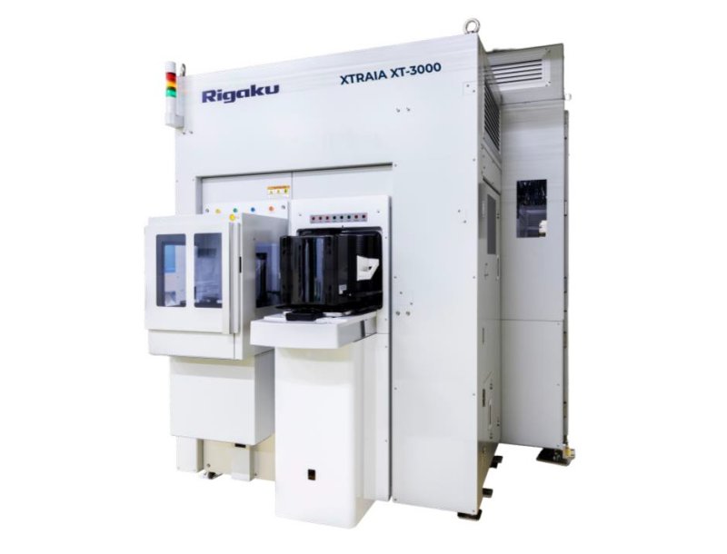
XTRAIA XT Series (Fab)
- Fully automated, cleanroom-ready system
- SECS/GEM and GEM300 integration for fab connectivity
- Wafer OCR and automated transfer for 75–300 mm wafers
- ISO Class 6 clean-level equivalent with FFU compliance
- Designed for high-volume manufacturing QC

Contact Us
Whether you are interested in getting a quote, want a demo, need technical support, or simply have a question, we're here to help.