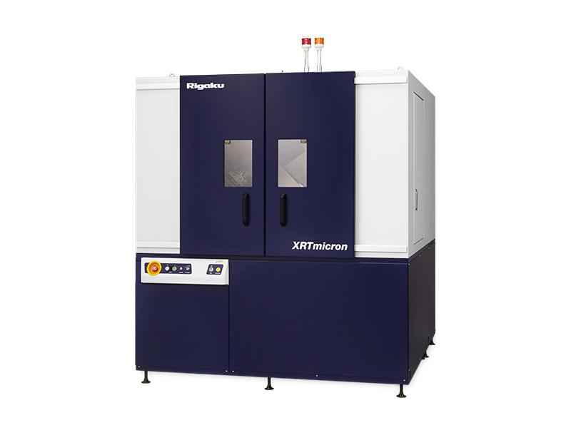
XRTmicron
Features
  • High-brilliance dual-wavelength X-ray source: MicroMax-007 DW
  • High resolution CCD camera: XTOP (5.4 μm pixels)
  • Ultra-high resolution CCD camera: HR-XTOP (2.4 μm pixels)
  • Horizontal sample mount for minimum artificial strain to wafers
  • Automatic wafer curvature correction for best dislocation image quality
  • Automated system operation including X-ray anode switch, detector switch, optics switch and alignment, sample alignment, and image collection
  • Automated dislocation analysis
  • 3, 4, 6, 8, 12 inch wafers supported
  • Wafer loader compatible

X-ray topography imaging system

For non-destructive evaluation of single-crystalline materials

Non-destructive dislocation imaging

Rigaku XRTmicron is a fast, high-resolution laboratory X-ray topography system for non-destructive dislocation imaging. Various types of dislocations and non-uniformity within single crystal wafers (such as Si, SiC, GaN, Ge, GaAs, quartz, sapphire, rutile, calcium fluoride etc.) can be imaged across wafers up to 300 mm in diameter. X-ray topography is a widely used dislocation analysis technique for both research and development and process control by various single crystal, wafer and device manufacturers.

Topography engineered for performance

Unmatched scan speed ten times higher compared to that of conventional systems is achieved by combining a high-brilliance dual-wavelengths X-ray source, the MicroMax-007 DW, and X-ray mirrors optimized for the topography application. Both Cu and Mo X-ray anodes and their mirrors are simultaneously mounted on the system and switched on-demand to perform reflection and transmission measurements without any system reconfiguration. A digital image of dislocations is captured by a either a high resolution (5.4 μm pixels) or ultra-high resolution (2.4 μm pixels) CCD camera. Both cameras can be simultaneously mounted on the system and switched on-demand depending on the required resolution.

Fully automated X-ray topography

Engineered for usability, the entire data image collection process - including anode switch, detector switch, optics switch and alignment, sample alignment and image collection - is fully automated. Furthermore, the system can be combined with a wafer loader and image recognition based dislocation counting software. Customized recipes can be built to automate the entire process from loading a wafer to reporting dislocation densities.

Specifications
Product name XRTmicron
Technique X-ray topography
Benefit Non-destructive evaluation of single-crystalline materials
Technology Imaging using X-rays
Core attributes High-flux multi-target X-ray source, CCD imager
Core options XTOP or HR-XTOP CCD
Computer External PC, MS Windows® OS, 
Core dimensions 1800 (W) x 1800 (H) x 1870 (D) (mm)
Mass (core unit) 2200 kg
Power requirements 3Ø, 200 V, 15 A 

XRT Publications

  1. Thomas Wicht et al,: “X-ray characterization of physical-vapor-transportgrown bulk AlN single crystals” Jour. Appl. Cryst., vol.53, (2020) 1080 – 1086 https://journals.iucr.org/j/issues/2020/04/00/te5057/te5057.pdf
  2. T. Abe et al,: “Steady distribution structure of point defects near crystal-melt interface under pulling stop of CZ Si crystal” Jour. Cryst. Growth, vol.459, (2017) 87 – 94 https://www.sciencedirect.com/science/article/pii/S0022024816307849
  3. Tanaka et al,: “Growth of Shockley type stacking faults upon forward degradation in 4H-SiC p-i-n diodes” Jour. Appl. Phys., vol.119, (2016) 095711-1 – 095711-9 https://aip.scitation.org/doi/abs/10.1063/1.4943165
  4. Fraunhofer Institute for Integrated Systems and Device Technology IISB: https://www.iisb.fraunhofer.de/en/press_media/press_releases/pressearchiv/archiv_2019/rigaku_xrtmicron_2019.html
  5. Yonenaga and K. Kutsukake: “Transmission behavior of dislocations against Σ3 twin boundaries in Si” Jour. Appl. Phys., vol.127, (2020) 075107-1 – 075107-8 (XRT-300) https://aip.scitation.org/doi/abs/10.1063/1.5139972
  6. N. Shinagawa et al,: “Populations and propagation behaviors of pure and mixed threading screw dislocations in physical vapor transport grown 4H-SiC crystals investigated using X-ray topography” Jpn. J. Appl. Phys., vol.59, (2020) 091002-1 – 091002-7 (XRT-100+HR-XTOP) https://iopscience.iop.org/article/10.35848/1347-4065/abab46/meta
  7. N. Tatsumi et al,: “Crystalline quality distributions of the type IIa diamond substrate and the CVD diamond layer processed by chemical mechanical polishing using a SiO2 wheel” Jpn. J. Appl. Phys., vol.57, (2018) 105503-1 – 105503-6 (XRT-300) https://iopscience.iop.org/article/10.7567/JJAP.57.105503/meta
  8. K. Inaba : “Defect structure analysis in single crystal substrates using XRTmicron” Rigaku Journal, vol.36 no.2, (2020) 11-18 https://www.rigaku.com/journal/summer-2020-volume-36-no-2/11-18
  9. New products “Automated dislocation evaluation software for X-ray topography images” Rigaku Journal, vol.32 no.1, (2016) 33-35 https://www.rigaku.com/journal/winter-2016-vol32-no1/33-35
  10. New products “High-throughput, high-resolution X-ray Topography imaging system” Rigaku Journal, vol.30 no.1, (2014) 30-32 https://www.rigaku.com/journal/winter-2014-volume-30-no-1/30-32
  11. K. Omote : “Crystal defects in SiC wafers and a new X-ray Topography system” Rigaku Journal, vol.29 no.1, (2013) 1-8 https://www.rigaku.com/downloads/rigaku-journal?page=7