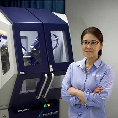
Presenter: Dr. Shyjumon Ibrahimkutty
High-resolution X-ray diffraction is a versatile and powerful tool in semiconductor materials and devices. Quick and non-destructive characterization of thickness, composition, quality, orientation, lattice strain, etc. are possible by XRD. This webinar will cover different high-resolution optics available for the SmartLab diffractometer for the basic and sophisticated characterization of epitaxial layers. Various high-resolution techniques such as rocking curve, reciprocal space map etc. will be discussed.

Contact Us
Whether you're interested in getting a quote, want a demo, need technical support, or simply have a question, we're here to help.

Subscribe to the Bridge newsletter
Stay up to date with materials analysis news and upcoming conferences, webinars and podcasts, as well as learning new analytical techniques and applications.
