XRF, XRD and XRR for thin film characterization
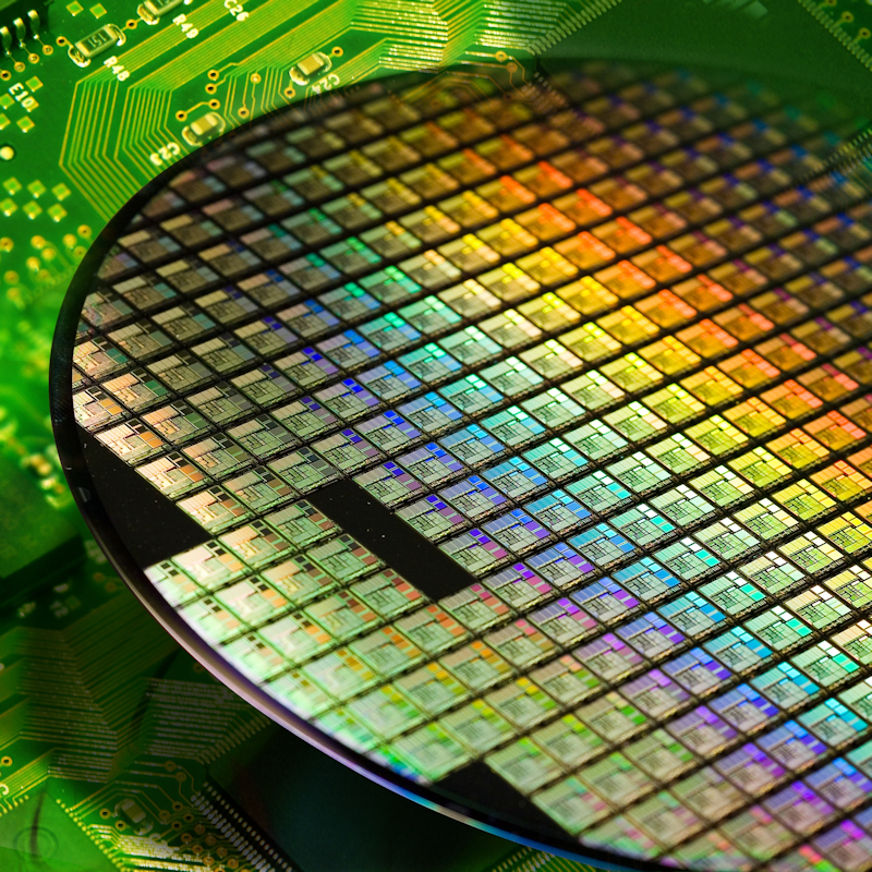
Within the semiconductor industry, there is a continual demand for integrated circuits (IC) that exhibit higher performance at a lower cost than its predecessors. Wafer metrology tools are used to design and manufacture ICs by carefully controlling the film properties, linewidths, and potential defect levels in order to optimize the manufacturing process of these devices. Metrology tools combined with wafer inspection capabilities are able to ensure that they target physical and electrical properties of semiconductor devices under production. Wafer metrology is able to specifically identify surface particles, pattern flaws, and other conditions that could cause adverse effects to the performance of these devices.
Rigaku is a pioneer and world leader in designing and manufacturing X-ray based measurement tools (X-ray diffraction, X-ray fluorescence and X-ray reflectometry) to solve semiconductor manufacturing challenges. With about 30 years of global market leadership in the semiconductor industry, our families of products enable everything from in-fab process control metrology to R&D for thin film and materials characterization.
Application notes
The following application notes are relevant to this applicationXRD
Rigaku recommends the following systems:
X-ray topography (XRT)

A fast, high-resolution laboratory X-ray topography system for non-destructive dislocation imaging
SAXS

A modernized 2D Kratky system that eliminates data corrections required of traditional systems
XRD

Advanced state-of-the-art high-resolution XRD system powered by Guidance expert system software
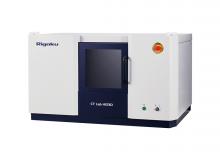
X-ray CT
Semiconductors
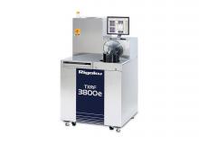


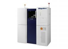
Ultra-trace elemental surface contamination metrology by TXRF with VPD capability; up to 300 mm wafers
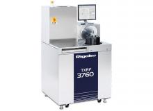
In-line, simultaneous WDXRF spectrometer for wafer metal film metrology; up to 300 mm wafers
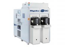
Sequential WDXRF spectrometer for elemental analysis and thin-film metrology of large and/or heavy samples

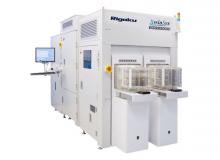
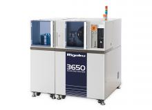
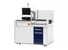
Process XRR, XRF, and XRD metrology tool for blanket and patterned wafers; up to 300 mm wafers